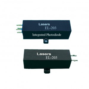
Drive circuit 3
Drive circuit 3
Parameters
|
Parameters |
Specification |
|
Driving current |
40~70A |
|
Driving voltage |
No more than 5V |
|
Discharge frequency |
No more than 5Hz |
|
Power supply mode |
DC 18V-36V |
|
Trigger mode |
Internal/external trigger |
|
External interface |
Opto-isolator, rising edge trigger |
|
Pulse width(Electric discharge) |
1ms~4ms |
|
Rising/falling edge |
≤15us |
|
Current stability |
≤5% |
|
Driving control |
RS485 |
|
Storage temperature |
-55~85°C |
|
Operating temperature |
-40~+65°C |
|
Dimension(mm) |
70*38*28 |

1) Description
|
1 |
24V power input |
|
2 |
Connect to lasers |
|
3 |
Controlling interface |
2) Definition
|
PIN |
|
|
|
1 |
SG+ |
External trigger+ |
|
2 |
SG- |
External trigger- |
|
3 |
RS+ |
RS485+ |
|
4 |
RS- |
RS485- |
|
5 |
GND |
RS485GND |
1)USART: RS-485
2)Baud rate : 115200bps
3)From: 8 date bits(a start bit,a stop bit, no parity)
4)Least significant byte is transmitted first (lsb)
5)Message format:
|
Header(1 byte) |
|
Message |
|
End(1 byte,checksum) |
Table1: Header description
|
Byte name |
Byte type |
Byte length |
values |
Note. |
|
Start coding |
unsigned byte |
1 |
0xAA |
Constant |
Table2: End(checksum) description
|
Byte name |
Byte type |
Byte length |
values |
Note. |
|
Checksum |
unsigned byte |
1 |
0-255 |
Total bytes(header and end) divided by 256, taking the reminder. |
1)Data output
Main control panel sends orders to array drive. An order includes 5 bytes which consists of 3 bytes of message(message bytes can be added or deleted)
Table 3:Data output
|
Order |
Byte1 |
Byte2 |
Byte3 |
Note. |
|
Internal/external trigger status |
0X01 |
0X00=external trigger 0X01=internal trigger |
0X01 |
Normally, external trigger is applied to use Internal triggers can be used for debugging |
|
Output current setting |
0X02 |
0X00 |
Current |
Range: 40~70A step size1A |
|
Output pulse width setting |
0X03 |
High byte pulse-width |
Low byte pulse-width |
Range: 1000~4000us step size:1us |
|
internal clock |
0X04 |
0X00 |
Frequency |
|
|
LD data saving |
0X09 |
0X00 |
0X01 |
|
|
LD output start/stop |
0X07 |
0X00=stop 0X01=start |
0X01 |
2)Data input
Array drive sends messages to main control panel.
Response latency:1000ms. Within response latency time, if main control panel doesn’t receive messages from array drive, there must be error. A message includes 5 bytes which consists of 3 bytes of message
Table 4:Data input
|
Order |
Byte1 |
Byte2 |
Byte3 |
|
Internal/external trigger status |
0X01 |
0X00=external trigger 0X01=internal trigger |
0X01 |
|
Output current setting |
0X02 |
0X00 |
Current |
|
Output pulse width setting |
0X03 |
High byte pulse-width |
Low byte pulse-width |
|
Internal clock |
0X04 |
0X00 |
Frequency |
|
LD data saving |
0X09 |
0X00 |
0X01 |
|
Self-adaptive LD voltage |
0X05 |
0×00 |
0×00 |
|
LD output start/stop |
0X07 |
0X00=stop 0X01=start |
0X01 |
|
LD over-current error |
0X0A |
0X00 |
0X01 |
|
Charging-voltage excess |
0X0B |
0X00 |
0X01 |