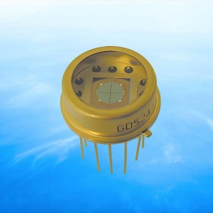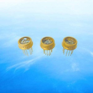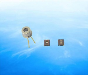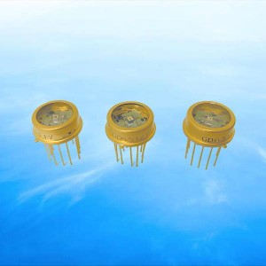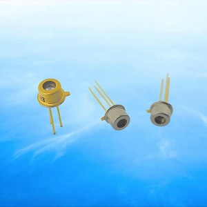


905nmAPD single tube series


|
Photoelectric characteristics (@Ta=22±3℃) |
|||||||||
|
Model |
GD5210Y-2-2-T046 |
GD5210Y-2-5-T046 |
GD5210Y-2-8-T046 |
GD5210Y-2-2-LCC3 |
GD5210Y-2-5-LCC3 |
GD5210Y-2-2-P |
GD5210Y-2-5-P |
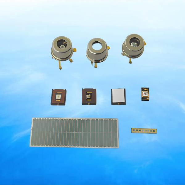
Array |
|
|
Package form |
TO-46 |
TO-46 |
TO-46 |
LCC3 |
LCC3 |
plastic packaging |
plastic packaging |
PCB |
|
|
Photosensitive surface diameter (mm) |
0.23 |
0.50 |
0.80 |
0.23 |
0.50 |
0.23 |
0.50 |
customized |
|
|
Spectral response range (nm) |
400~1100 |
400~1100 |
400~1100 |
400~1100 |
400~1100 |
400~1100 |
400~1100 |
400~1100 |
|
|
Peak response wavelength (nm) |
905 |
905 |
905 |
905 |
905 |
905 |
905 |
905 |
|
|
Responsiveness λ=905nm Φ=1μW M=100 (A/W) |
55 |
55 |
55 |
55 |
55 |
55 |
55 |
55 |
|
|
Dark current M=100(nA) |
Typical |
0.2 |
0.4 |
0.8 |
0.2 |
0.4 |
0.2 |
0.4 |
According to photosensitivity |
|
Maximum |
1.0 |
1.0 |
2.0 |
1.0 |
1.0 |
1.0 |
1.0 |
One side |
|
|
Response time λ=905nm R1=50Ω(ns) |
0.6 |
0.6 |
0.6 |
0.6 |
0.6 |
0.6 |
0.6 |
According to photosensitive surface |
|
|
Working voltage temperature coefficient T=-40℃~85℃(V/℃) |
0.9 |
0.9 |
0.9 |
0.9 |
0.9 |
0.9 |
0.9 |
0.9 |
|
|
Total capacitance M=100 f=1MHz(pF) |
1.0 |
1.2 |
2.0 |
1.0 |
1.2 |
1.0 |
1.2 |
According to photosensitive surface |
|
|
breakdown voltage IR=10μA(V) |
Minimum |
130 |
130 |
130 |
130 |
130 |
130 |
130 |
160 |
|
Maximum |
220 |
220 |
220 |
220 |
220 |
220 |
220 |
200 |
|
Front Plane Chip Structure
High speed response
High gain
Low junction capacitance
Low noise
Array size and photosensitive surface can be customized
Laser ranging
Lidar
Laser warning